

Considerations in SMT Assembly
In a world that increasingly demands sustainable and eco-friendly electronics, manufacturers need to prioritize environmental considerations in Smt assembly. This means incorporating eco-friendly processes, adopting lead-free soldering and minimizing energy consumption. These measures are not only necessary to comply with regulations but also to appeal to environmentally conscious consumers.
The smt assembly process is a multi-step one that involves many steps of etching, drilling, and soldering. It can generate a lot of dust and emissions that may pollute the surrounding environment. Therefore, it is important to have a good ventilation system in the factory that can effectively control and minimize such pollutants.
An effective PCB protective coating can help prevent moisture, chemicals, and other contaminants from damaging the board. Such coatings are essential in electronic devices that need to withstand harsh environments, such as aerospace and automotive.
PCBs are usually made of a non-conductive material, such as fiberglass or plastic. Copper traces on the surface act as pathways for electrical currents, and are etched using photolithography processes. This step is followed by precision drilling to create holes for component mounting and interconnection of different layers in multi-layer PCBs. A thin layer of metal is then deposited on the walls of drilled holes and exposed copper surfaces to enhance solderability.
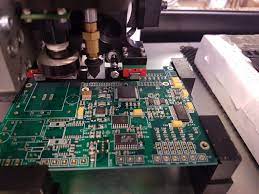
Next, automated pick-and-place machines place the individual components onto the circuit board. Thorough inspection and testing throughout the process ensures that all components are properly placed. Automated optical and X-ray inspections are key for identifying errors such as soldering defects. Using a high-quality conformal coating can also enhance the durability of a circuit board, allowing it to withstand harsh environmental conditions and extend its lifespan.
Environmental Considerations in SMT Assembly
Once the finished product is ready, the manufacturing process can also cause a significant amount of waste and emissions. Responsible disposal and recycling of materials can minimise these negative effects. Efficient logistics management and the use of low-emission transportation options can also reduce carbon footprints.
While it is possible to manufacture a circuit board using green technologies, it is even better to design it from the outset using sustainability principles. This includes selecting eco-friendly materials, reducing the size of components and ensuring that they are easily disassembled and recycled at the end of their life cycle.
An experienced contract electronics manufacturer should be able to offer comprehensive environmental testing for their PCB assemblies. This testing can simulate a range of environmental factors to test whether the product will function correctly in these conditions. This is a specialist process that should only be carried out by an expert contractor with the right in-house facilities. This type of testing is vital to the reliability, safety and performance of your product, so it is worth investing in an expert that can provide this service.
An additional benefit of environmental testing is that it can identify potential issues before they become costly or dangerous. This can save you time, money and stress in the long run. Aside from the benefits outlined above, choosing a PCB manufacturer that carries out environmental testing can also improve your chances of winning a contract.